Line Scan Camera Vision System Imitator
Jul 01, 2009
Emulating a Line Scan Camera Image Default Detection System in Software
Project Summary:
Software to Emulate Line Scan Camera Image Default Detection System
Background Rationale
I was employed at Schenk Vision in 2008 and 2009, a company that creates optical inspection equipment for all sorts of flat materials, as shown below.
 Image Credit Schenk Vision
Schenk Vision is a German Company, based in Munich, Bavaria. Germany is known for its high precision optics and many interesting small to medium sized engineering and production companies with extremely high end and niche applications that sell globally. I was fortunate enough to work for Schenk Vision as an Optical Applications Engineer and get a bit of an inside view on how their system works. Though my background is in Computer Engineering, there isn’t really a common University discipline or Bachelors Degree specifically for, “Optical Engineering,” so typically these types of jobs default to Electrical Engineers, Computer Engineers or perhaps those with degrees in Physics. I qualified because I had spent a lot of my undergraduate degree working with LED lights, power electronics and nerded out over the vagaries of the physics of lighting, LED datasheets, lens specifications and the like.
During my first week on the job, I was handed a copy of an Optics textbook, which I later bought a copy of my own and still own today, and was told to read it, which I did. As a result of reading this book and working at Schenk Vision I received a highly unique education on optics early in my career.
The way Schenk Vision accomplishes high-speed, roll-to-roll inspection is by taking images through a proprietary camera called a, “line scan camera,” which is essentially a digital camera with a two-sensor-pixel wide charged-coupled device (CCD). So basically, the CCD is a very long rectangle rather than a typical square. The reason two sensor-pixels are required on a CCD for this application rather than one is essentially for “reproducibility.” Both pixels capture light from photons coming off of the back of a spherical lens, and the average output voltage of those two sensors becomes one pixel on a digital image. This way if there are any extremely slight aberrations on the lens from its original manufactured state, it won’t have as much impact on the final digital image from camera to camera.
The CCD sits behind a camera lens, the same type of round off-the-shelf lens that a photographer might use with his or her square CCD. That lens points at some kind of moving flat surface - whether it be glass or plastic film or some kind of metal, and the line scan camera takes picture after picture on a continuous basis, with software stitching those line-by-line images into one big long, “square photograph,” on the back end. LEDs provide a source of light, typically in the red spectrum, because the CCDs are designed to pick up the widest range of red light, but the color could be customized based upon the material if necessary.
All of this is happening in real time, so of course the software that stitching the images together can also be programmed to look for different anomalies, taking advantage of the minute differences in the surface material and how that material either reflects, diffuses or scatters light from the surrounding, “normal,” material around it.
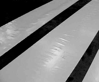 Example of Defect on Roll Plastic - Image Credit Plastics Technology
Now, you might be asking - why don’t you use a, “flat” lens as well as a line scan camera? The reason is because circular, regular lenses are 1) Easier to produce, cheaper and already exist and 2) the way lenses are constructed and focus on an object is through rotational mechanical adjustment, which allows an extreme amount of precision, down the the micron. Using some kind of linear lens would make that adjustment incredibly difficult.
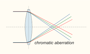 Illustration of how lenses translate photons from one surface size to a smaller surface size using refraction. Note that different wavelengths of light reflect at different angles given the same material, known Dispersion.
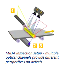
The web detection setup in production looks something like this:
My task as optical applications engineer was to take samples and materials mailed to us by customers and determine in a lab whether the Schenk equipment would work in a production environment.
This involved using a simple lab setup with variable speed, a single line scan camera and a lot of time, patience and interestingly enough…a lot of tape.
The output of the lab setup was an actual .png image, saved to a desktop PC, which previous to my having worked there, would have been inspected visually by someone on staff, who would have made a guess whether the inspection was feasible based upon past experience. My thought was: rather than guess as to whether a defect could be detected, why not write software that would measure and tag the images directly, mimicking precisely what the German-designed in-house software does?
Benefit and to Whom
This was a direct benefit to my employer at the time, Schenk Vision.
Project Status or Outcome
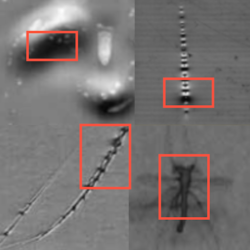
Typical in-process defects show up on the output screen in a manner shown below. Flat surfaces are imaged, displaying shadows or bright spots in various shapes.
There are six main ways that radiation interacts with materials:
- Transmission
- Reflection
- Refraction
- Diffraction
- Absorption
- Scattering
Actually, diffraction is really just a function of refraction, scattering is a function of reflection and transmission is simply refraction twice, through two surfaces. So really there are three ways that radiation interacts with materials:
- Refraction
- Absorption
- Reflection
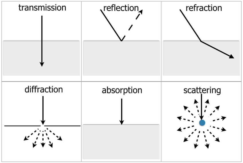
When you have a bump or a valley on a material, even if that bump or valley is extremely minute, sometimes not even visible by the human eye at speed or from a distance, it reflects or refracts light in different directions than the rest of the material. On the line scan camera, this results in an either white or dark pixel, as shown in the below example image up close:

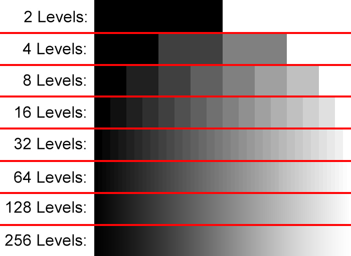
Basically, the pixels stored within the image are stored as a series of interlaced values, with the values from 0 to 255 representing 8-bit grayscale brightness levels, like so:
1 6 4 6 2 6 4 6
7 7 7 7 7 7 7 7
5 6 5 6 5 6 5 6
7 7 7 7 7 7 7 7
3 6 4 6 3 6 4 6
7 7 7 7 7 7 7 7
5 6 5 6 5 6 5 6
7 7 7 7 7 7 7 7
This interlacing method is all documented in the web standard specification for PNG images. “Grey Levels,” are essentially gradients on an image allowing color to be represented. PNGs can be specified at 8-bit, which was what the Schenk system used, and this could be mapped out in image processing software that I built within a coding language and mathematical development environment I used called, “Matlab.”
Using Matlab, I was able to successfully create a program that input .png images from the lab equipment, and output PDF reports that would identify defects based upon user-defined size, shape and deviation from mean brightness parameters.
In combination with this software and lab-know how, Schenk was able to improve response time and accuracy to customers, along with a professional, automatically PDF report which built confidence in the customers’ minds that we would be able to do the job.